SEATTLE–(BUSINESS WIRE)–ATREG, Inc. which specializes in helping advanced technology companies divest and acquire infrastructure-rich manufacturing assets (semiconductor fabs and cleanrooms) worldwide, announced today that the acquisition of onsemi’s operational 200mm manufacturing fab located in Pocatello, Idaho, USA by LA Semiconductor has officially closed. Established in 2022 by Tallmadge, OH-based Linear ASICS, Inc., LA Semiconductor is the newest U.S.-owned and -operated, fully operational 180nm-capable pure-play semiconductor foundry for analog, mixed signal, and power products.
Located on a 33-acre campus with over 50,000 square feet of cleanroom space and over 550,000 square feet of building space, the Pocatello fab currently produces 0.35 µm to 1.5 µm analog CMOS, BCD, advanced discrete, and custom technologies.
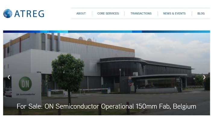
“In addition to our South Portland, Maine and our Oudenaarde, Belgium fabs, this is the third manufacturing asset disposition that ATREG has helped us with over the past 12 months,” explains Wei-Chung Wang, executive vice president, global manufacturing and operations for onsemi. “This divestment is a continuation of onsemi’s fab-liter manufacturing strategy aimed at achieving a sustainable financial performance through upscaling capacity for products in our key markets of automotive and industrial.”
“ATREG’s working relationship with onsemi dates back to the mid-2000s and we truly appreciate onsemi’s leadership’s trust in the ability of our team to assist with these types of assignments,” adds Stephen Rothrock, founder, president and CEO of ATREG. “We are pleased to have made a significant contribution to onsemi’s global manufacturing strategy over the course of so many years.”
About ATREG, Inc.
Headquartered in Seattle, USA, ATREG, Inc. specializes in helping global companies divest and acquire infrastructure-rich advanced technology manufacturing assets, including front-end and back-end semiconductor fabs, cleanroom facilities, and technology campuses in North America, Europe, and Asia. For more information, please visit our web site, read our blog, or follow us on LinkedIn and Twitter.